
Samsung presented the 3D memory concept models zHBM and zNAND-O at the FMS 2026 conference: in the first, HBM stacks are built vertically directly above the AI accelerator, rather than placed next to it, while the second brings HBM-like memory to on-device AI scenarios. The company claims a several-fold increase in performance, energy efficiency, and density, but both developments remain prototypes without announced release dates. The tangible part of the announcement is the roadmap for serial memory, from HBM4E to V10 BV-NAND.

What Happened
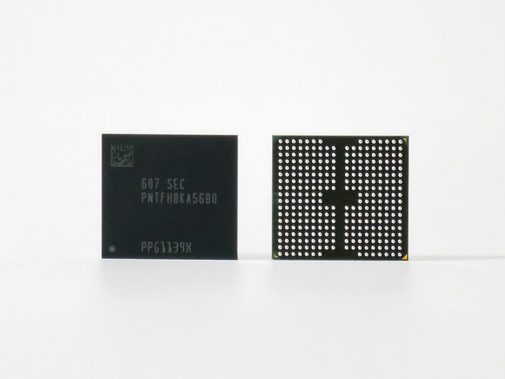
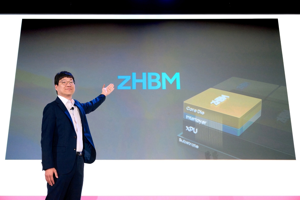
At the Flash Memory Summit 2026, held in Santa Clara from August 4 to 6, Samsung presented the industry's first 3D memory concept models. The first, zHBM, is an architecture in which HBM is stacked along the z-axis directly above the AI accelerator (xPU), rather than placed next to it. The second, zNAND-O, is NAND flash with an HBM-like structure, similar to the HBF direction being developed by SK hynix and Sandisk; it is designed for on-device AI and was shown in 4- and 8-layer configurations based on TSV technology. According to Samsung, the interface with zHBM provides up to an 8-fold increase in data processing compared to 8th-generation HBM5, a threefold increase in performance per watt, a reduction in thermal resistance of more than 50%, and, when using the new wafer bonding technology, up to 10x memory density compared to HBM5. As part of the same presentation, the company showed V10 BV-NAND with more than 400 layers (density approximately 58% higher than V9) and a roadmap that included HBM4E, HBM5, LPDDR5X-PIM, and enterprise SSDs PM1763 and BM1773.
Context
A key limitation of modern AI systems is not only the accelerators themselves, but also memory: between the chip and the HBM stacks, which traditionally lie on the substrate next to it, there is a constantly growing flow of data that consumes energy and turns into heat. Memory bandwidth, power consumption, and heat dissipation are most often cited as the main bottlenecks for training and inference of large models, so the question of physical memory placement has long ceased to be an engineering detail. The comparison base chosen by Samsung is also telling: the claimed figures are given against HBM5 — a generation that has not yet entered mass production, meaning the benchmark is set one step ahead of the current market, not on it.
Why This Matters for the Industry
For the industry, zHBM is a claim to a new integration scheme: moving memory from an adjacent substrate directly above the accelerator shortens the data path and thereby attacks three bottlenecks of AI systems at once — bandwidth, power consumption, and heat dissipation. The ability to embed client IP blocks in the interlayer between memory and xPU points to a trend of co-designing memory and accelerators for specific AI workloads: chip manufacturers and system assemblers gain a degree of integration that does not exist today. At the same time, zNAND-O places Samsung in the same league as SK hynix and Sandisk in the race for HBF-like NAND for peripheral AI. For builders, this is a signal of the agenda, not an available capability: there is no access to zHBM and zNAND-O, no APIs or SDKs, and it is impossible to build a product on them; the working benchmarks now are the roadmap items, primarily HBM4E and HBM5, as well as the advancement of V10 BV-NAND.
Why This Matters for Users
If zHBM makes it from prototype to mass production, the architecture of training and inference systems will change: more bandwidth with less heat dissipation means that the same models can be served faster and cheaper, and more compute fits in a rack. For end users, this translates into more responsive and less expensive AI services. A separate line is zNAND-O and on-device AI: memory with an HBM-like structure opens up scenarios in which models run locally, on the device itself, without recourse to the cloud. A practical checklist for monitoring the story consists of three tracks: the status of zHBM and zNAND-O, the mass production of HBM4E and HBM5, and the advancement of V10 BV-NAND.
What Is Still Unknown / Limitations
zHBM and zNAND-O were shown as concept prototypes: commercialization timelines have not been announced, and there are no specifications, prices, or latency data. All key figures are vendor claims without independent measurements, and reproducible metrics were not published in the conference materials, so it is practically impossible to verify them in the near future. Currently, only dated events are verifiable in the story: the supply of HBM4E samples to customers began in May 2026. Left out of the frame were the yield metrics for wafer bonding and the thermal regimes of vertical assembly — it is precisely these that will determine whether the concept reaches mass production.
Sources
- Samsung Global Newsroom — Samsung Unveils Next-Gen 3D-Memory Vision at FMS 2026
- Samsung Semiconductor Newsroom — Inside FMS 2026: Samsung Electronics Showcases the Future of AI Memory
- The Elec — report from FMS 2026 on Samsung's presentation
Author
Look at AI, editorial team