SK hynix has outlined how the memory hierarchy will evolve to meet AI demands: the HBM line will continue through HBM4E, custom HBM with customer logic will appear, DRAM will be placed directly on accelerator dies, and NAND flash will take on a new role as the HBF tier. The company describes the shift as moving the AI system bottleneck from compute to memory: by 2030, memory requirements could grow many times over.

What happened
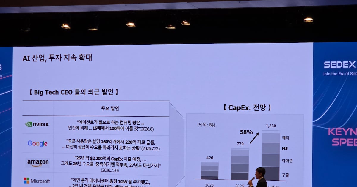
On October 14 at SEDEX 2026 in Seoul, SK hynix CDO Ahn Hyun presented a memory development roadmap designed for growing AI workloads. The company announced continued HBM development through HBM4E, expansion of custom HBM where customers can place their own logic in the base die, and work on 3D Stacked DRAM — a technology for placing DRAM directly on GPUs and NPUs. A separate item was the HBF (High Bandwidth Flash) announcement: TSV-stacked NAND flash positioned as a memory hierarchy tier between HBM and SSD, with target specs of roughly half the bandwidth of same-generation HBM at approximately 10x capacity. SK hynix estimates AI infrastructure performance requirements will grow ~20x by 2030 relative to 2026 levels; Chosun Biz cites a 109% CAGR over that period. The company links the requirement growth to expanding KV caches, context lengths, and inference request volumes.
Context
To understand the significance of this step, it helps to recall how large-model inference works. Dialogue state is stored in the KV cache, whose size grows with context length and concurrent session count, so in agentic scenarios memory is consumed faster than compute resources. The memory hierarchy still has gaps: on-chip SRAM on accelerators is small in capacity, HBM is fast but expensive and limited in volume, and standard SSDs are too slow for active model work, with these gaps currently compensated by software logic. SK hynix's roadmap reads as a plan to fill these gaps with hardware tiers — a memory tier on the accelerator itself and a fast flash tier for large data volumes. The commitment to standardize HBF through OCP jointly with SanDisk additionally signals that the new memory class is intended as open and available to the entire ecosystem, not a closed single-vendor solution.
Why this matters for the industry
For the industry, this is a signal to change basic planning assumptions: memory becomes a limiter of AI infrastructure on par with compute, and the next generations of accelerators and data centers will be designed with the stated hierarchy in mind. Custom HBM with customer logic in the base die opens a surface for co-design of memory and accelerator, expanding the architectural solution space for all chip vendors. If HBF's bandwidth-to-capacity ratio is confirmed, it will become a natural carrier for cold KV-cache layers and batched inference, where capacity matters more than peak speed. Memory also moves to a price-setting factor for inference: unit economics should be recalculated with memory as a separate cost line, KV-cache growth and long-context costs should be profiled in own systems, and these metrics should be built into TCO models for the next procurement cycle. In this competition, those who build software around the new memory hierarchy are more likely to win than those who simply buy more GPUs. Infrastructure planning teams should additionally track OCP documents on HBF to see the formation of the new memory class specification in time.
Why this matters for users
For readers, the news partially explains why AI services are getting more expensive and why long contexts and heavy agentic sessions are price-limited: the bottleneck for such services is memory capacity and speed, and HBM shortages hit markets and service costs. No immediate product changes should be expected: this is a roadmap, not a device announcement, and there is nothing to buy or test today. The prospect is that with partial implementation of the plan, inference will become cheaper and more energy-efficient: scenarios currently blocked by VRAM capacity, such as very long agentic sessions and multi-million-token contexts, could become economically viable thanks to a flash tier with low cost per bit and DRAM placement closer to the accelerator.
What is still unknown / limitations
This is a roadmap, not a product announcement: as of October 14, 2026, sources contain no specific SKUs, prices, availability dates, latency measurements, or testing methodologies, so there is nothing to deploy or benchmark yet. HBF specs — roughly half HBM bandwidth at 10x capacity — are stated as targets, not measured results of a finished device. The composition of customer logic in the base die, its thermal and power requirements, software model, and evaluation methodology are not disclosed in sources. The 20x growth estimate by 2030 belongs to the vendor itself and is not supported by independent data. Sample timelines for 3D Stacked DRAM are not named, and HBF standardization through OCP is at an early stage, so conclusions about memory hierarchy restructuring timelines are premature.
Sources
- SK hynix Ahn says AI surges, drives Korea to develop 3D stacked DRAM and HBF — Chosun Biz
- SK Hynix Unveils Next-Generation Memory Roadmap to Address AI Bottlenecks — Korea IT Times
Author
Look at AI, editorial team